Electronic Fabrication & PCB Assembly Standards Guide
Master electronic fabrication processes including PCB baking, lead tinning, coil winding, CQFP preparation, and soldering standards for high-reliability.
Electronic Fabrication Processes
Assembly, Wiring, and Inspection Standards (Pages 12-28)
Process Assurance Division - Technical Refresher
Pre-Fabrication: Inspection & Baking
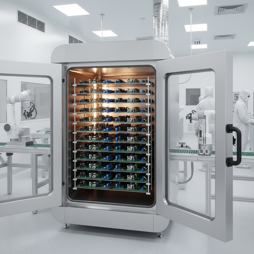
Before assembly begins, rigorous inspection and preparation are mandatory.<br><br><b>Visual Inspection:</b><br>• Verify QC approval for F/T clearance.<br>• Check for laminate defects, conductor defects, plating issues, and physical damage.<br><br><b>Bare PCB Baking Requirements:</b><br>• <b>General Baking:</b> 85°C ± 5°C.<br>• <b>For Reflow Soldering:</b> 120°C ± 5°C.<br>• <b>Duration:</b> 3 hours in Class 100 or Vacuum Oven.<br>• <b>Note:</b> Boards must not touch each other during baking.
Lead Preparation & Turret Swaging
<b>Lead Tinning:</b> Use a dross-free solder pot at 240-280°C. Dip leads with a withdrawal rate of 25 mm/sec and a dwell time of 2-3 seconds. Clean with IPA immediately after.
<b>Turret Swaging Critical Adjustment:</b> The distance between punch and anvil must equal the PCB thickness. Incorrect settings can damage the board.
<b>Proper Installation:</b> Bifurcated turrets must enter mounting holes freely. The punch should gently open the terminal into a funnel shape without splitting it excessively.
<b>Firm Fixation:</b> Ensure turrets are fixed firmly with no rotational movement.
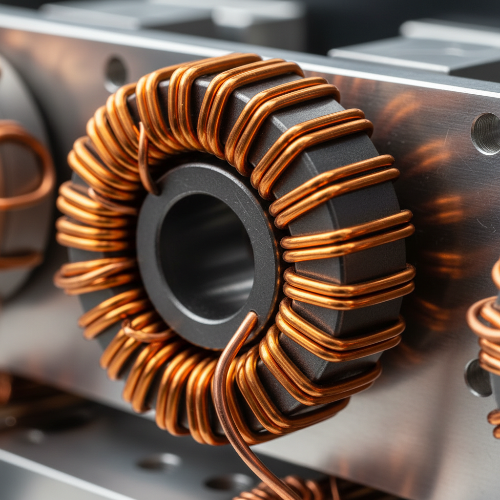
Coil Winding Procedures
Precise winding is required for subsystem reliability.<br><br><b>Single Winding Calculation:</b><br>(Single turn length × No. of turns) + 10% Overhead + 30cm Termination.<br><br><b>Bifilar Winding:</b><br>Fold wire into two equal halves and start winding from the folded end, leaving 15cm for termination.<br><br><b>Tagging & Testing:</b><br>Identify start/end with tags and dots. Use polyolefin shrinkable sleeves for insulation. All coils must undergo dry probe testing before assembly.
CQFP Component Preparation
<b>Visual Inspection:</b> Inspect CQFP for corrosion on leads, body damage, or lead deformation under magnification.
<b>Lead Tinning:</b> Dip leads in dross-free solder pot (240-280°C). Brush clean with IPA.
<b>Lead Forming Jig:</b> Set jig height to component thickness + 25 mils. Fix component flush with the cropping tool.
<b>Safe Handling:</b> Remove component from jig vertically upward to prevent bending the delicate formed leads.
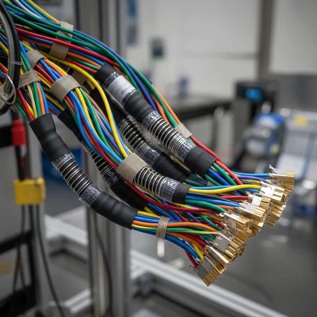
Specialized Wiring: PRT & 1553 Cables
<b>PRT Wiring:</b><br>• Clean lead wires with a surgical knife continuously at a 45° angle.<br>• Tin leads and protect with polyolefin sleeves (5mm diameter).<br>• Use Kapton conduits for insulation.<br><br><b>1553 Cable Shield Isolation:</b><br>• Strip outer jacket 10mm at connector side.<br>• Create a window 60mm from connector end.<br>• Loosen shield mesh, lift with tweezers, and insulate using polyolefin sleeves.<br>• Separate live and return paths with shrink tubing.
Connector De-Golding Process
<b>Purpose:</b> Removing gold plating from connector pins prevents brittle solder joints and ensures long-term reliability.
<b>Temperature:</b> Solder pot must be maintained at exactly 250°C.
<b>Procedure:</b> Dip pins into flux, then into molten solder for 2-3 seconds ("Double Dip" method often required).
<b>Post-Process:</b> Allow to cool for 2-3 minutes, then clean contacts via ultrasonic method using IPA.
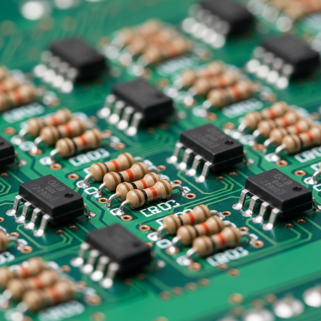
Component Mounting Standards
<b>General Rules:</b><br>• <b>Parallelity:</b> Components must be parallel to each other.<br>• <b>Flush Mounting:</b> Body must be in contact with PWB.<br>• <b>Stress Relief:</b> Radius of bend must be 3D to 6D.<br><br><b>Specifics:</b><br>• <b>Transistors (TO-39):</b> 1-1.5mm gap between lead seal and PWB surface.<br>• <b>ICs (DIP):</b> Body parallel to surface, lead protrusion 1-1.5mm on pattern side.<br>• <b>Relays:</b> Mechanically fixed by fastener; terminals electrically terminated by wiring.
Soldering Process Control
<b>Iron Maintenance:</b> Clean hot tip with wet sponge. Tin the bit during temperature buildup. Idle irons must have solder wiped before next use.
<b>Temperature Constraints:</b> Preferred range 240°C - 280°C. Never exceed 300°C.
<b>Technique:</b> Place iron to impart maximum heat to joint. Apply solder to the joint, not the iron. Allow solder to flow.
<b>Critical Rule:</b> "Never move the soldering iron over the joint." This prevents cold joints and disturbance.
Thermal Interfaces & Special Mounting
<b>Thermal Interface (Chotherm):</b><br>• Use Chotherm 1671 or 974 for axial lead components and DIP ICs.<br>• Material must be cut exactly to component length/width.<br>• Component leads are formed and placed over the Chotherm before soldering.<br><br><b>Turret Mounting:</b><br>• Components mounted on turrets must have a height of 1.2 to 1.5mm from turret base.<br>• Solder must not cover the component mountable hole area.
Capacitor Soldering & Stacking
<b>Ceramic Chip Capacitors:</b> Preheat at 100°C for 10 minutes. Solder without touching the delicate end caps (2-3 seconds duration).
<b>CWR 06 Capacitor Stacking:</b> Maximum stack height is 4 capacitors. Verify polarity using a jig.
<b>Adhesive Bonding:</b> Apply Epotek H74 to the non-terminal side interface. Cure at 150°C for 45 minutes.
<b>Soldering Stack:</b> Apply RMA flux to bottom cap. Ensure solder covers the junction properly. Clean residues with IPA.
- pcb-assembly
- soldering-standards
- electronic-fabrication
- circuit-board-inspection
- coil-winding
- surface-mount-technology
- industrial-manufacturing