
How Photolithography Shapes Semiconductor Wafers
Learn how photolithography prints billions of transistors onto silicon wafers using UV light, photoresist, and reticles in chip manufacturing.
Painting with Light
How Photolithography Prints the Brains of Our Devices
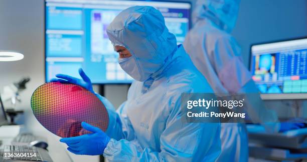
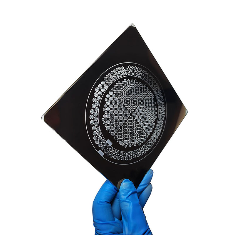
The Canvas: What is a Wafer?
A wafer is a thin slice of ultra-pure crystalline silicon.
It acts as the foundation (or canvas) for building electronic circuits.
Before we build, the surface must be polished to atomic smoothness.
The Impossible Scale
Modern chips have billions of transistors. Placing them one by one is impossible.
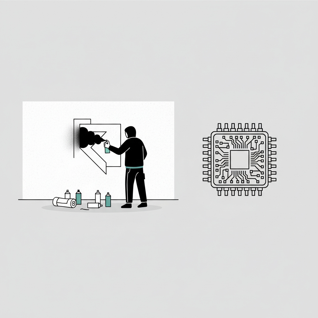
The Solution: A High-Tech Stencil
Instead of drawing every line, we use a process similar to stenciling or screen printing. We create a master pattern and copy it onto the wafer using light. This allows us to print billions of parts simultaneously.
What is Photolithography?
Photo = Light
Litho = Stone (Silicon)
Graphy = Writing
Literally: 'Writing on stone with light.'
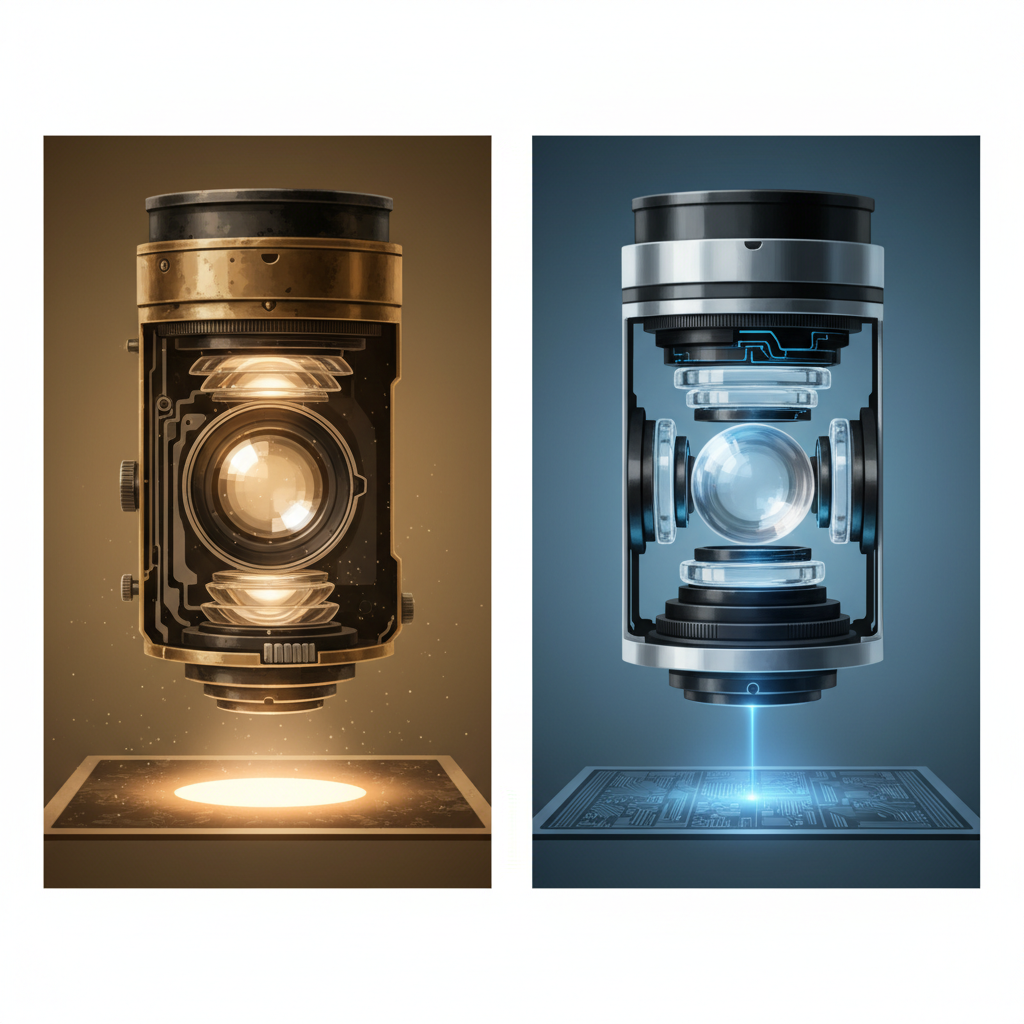
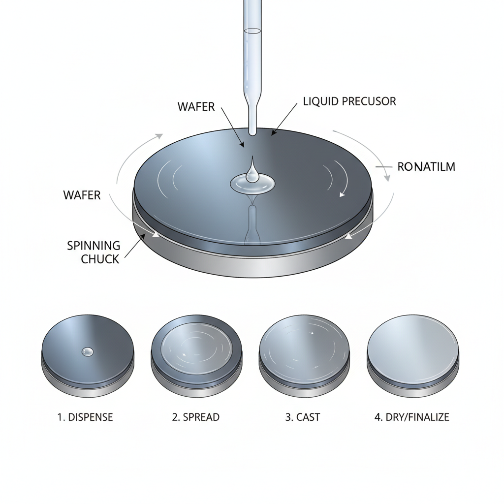
Step 1: The 'Film' (Photoresist)
Just like film in a camera reacts to light, we coat the wafer in a light-sensitive liquid called Photoresist.
Analogy: Think of it like spreading extreme sunscreen. Where the sun (UV light) hits, the chemistry changes.
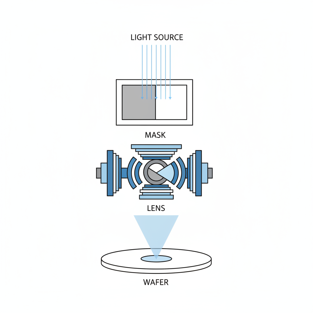
Step 2: The 'Blueprint' (Reticle)
We don't draw on the wafer. We draw on a quartz plate called a 'Reticle' or 'Mask' first. This is our master negative.
Light passes through transparent areas.
Chrome blocks light in other areas.
Step 3: Exposure (The Printing)
High-powered UV light is blasted through the mask.
Lenses shrink the image to 1/4th the original size for extreme precision.
The image is printed onto the photoresist on the wafer.
Why is this the ONLY way?
Speed: We print billions of transistors in seconds. Mechanical arms would take thousands of years.
Precision: Light creates features only a few atoms wide.
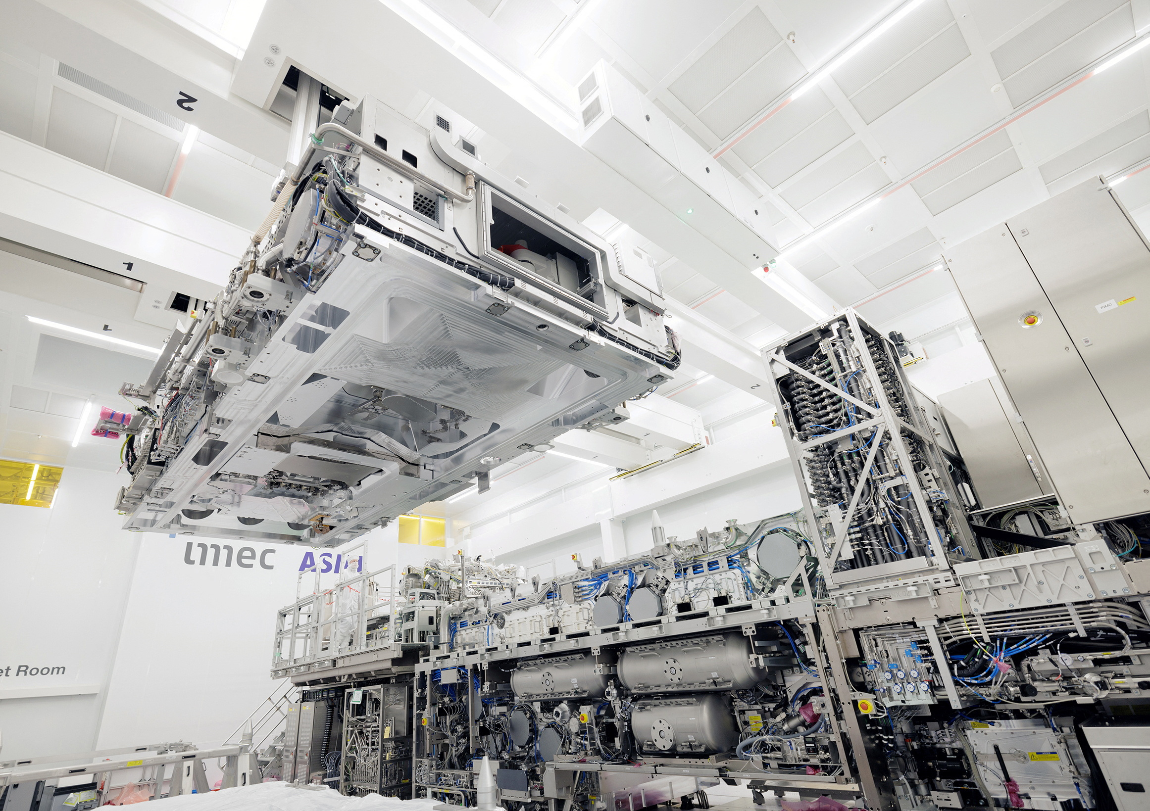
Pushing the Limit: EUV
To make chips faster, we need smaller patterns. We now use Extreme Ultraviolet (EUV) light.
The wavelength is just 13.5 nanometers. That's like writing with a pen tip the size of a DNA strand.
The Most Sophisticated Printing Press
Photolithography turns silicon into supercomputers.
It allows us to print circuitry smaller than a virus.
Without it, the modern digital world would simply not exist.
- photolithography
- semiconductor
- silicon-wafer
- chip-manufacturing
- euv
- electronics
- nanotechnology