Engineering Design of P-N Junction Solar Cells & Physics
Learn the materials, physics, and architecture of photovoltaic devices. Covers band gaps, V-I curves, Voc, Isc, and efficiency in solar cell engineering.
Engineering Design of P-N Junction Solar Cells
Materials, Physics, Architecture & Electrical Characteristics of Photovoltaic Devices
Semiconductor Engineering | Photovoltaic Systems
Silicon
GaAs
InAs
CdAs
Material Constants & Band Gap Analysis
Si
Silicon
1.12 eV
Most common PV material, dominating the global solar manufacturing industry.
GaAs
GaAs
1.42 eV
High efficiency III-V direct bandgap semiconductor, ideal for space and multi-junctions.
InAs
InAs
0.36 eV
Narrow band gap yielding strong IR absorption, useful for specialized sensors.
CdTe
CdTe (CdAs)
1.50 eV
Leading thin-film candidate offering low cost and excellent optical absorption.
Photon must have energy E_photon ≥ Eg to generate electron-hole pair
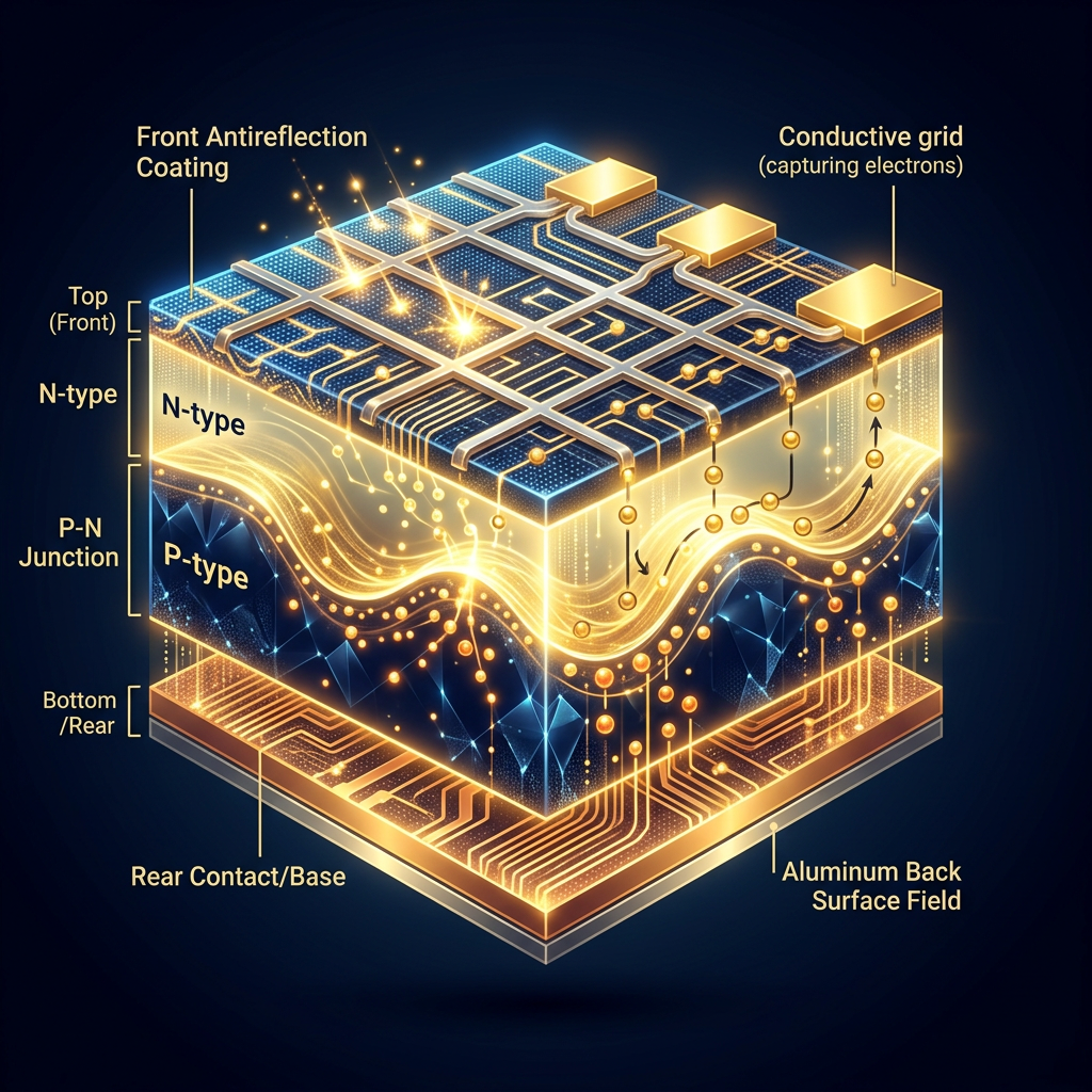
Device Architecture — Cross-Section Design
INCIDENT PHOTONS
GLASS WINDOW
Glass Window Layer
Anti-reflective protective layer that optimizes photon transmission.
Nickel Front Contact
Positive terminal (+) laid on the surface edges to minimize shading.
N-TYPE SILICON
N-type Silicon Layer
Ultra-thin, highly doped region favoring rapid electron collection.
Barrier Field
P-N junction depletion region generating internal electric field.
P-TYPE SILICON BASE
P-type Substrate
Thick base layer where the majority of photon absorption occurs.
METAL BACK CONTACT
Back Negative Contact
Negative terminal (−) providing uniform structural grounding.
Thin layers minimize minority carrier recombination before reaching junction.
Device Physics | Cross-Section Analysis
Physical Layout
Current Flow
Dimensional Engineering — Why Thin Layers Matter
The Diffusion Length Problem
1. Thin Region
2. Thick Region
Minority carriers generated far from junction recombine before contributing to current
P and N regions must be kept < diffusion length L = √(D·τ)
Recombination = loss of photogenerated current
Thin layers → higher collection efficiency → higher Isc
L = √(D·τ)
where D = diffusion coefficient, τ = carrier lifetime
Photovoltaic Mechanism
Photon Absorption & Carrier Generation
Photon Incidence
E_photon ≥ E_g = 1.12 eV (Si)
Bond Rupture
Valence electron freed
Pair Generation
Free carriers created
Carrier Separation
E-field sweeps carriers
Energy Band Model
Semiconductor Physics • Quantum Level Process
Sub-bandgap photons (E < E_g) do not generate pairs — absorbed as heat
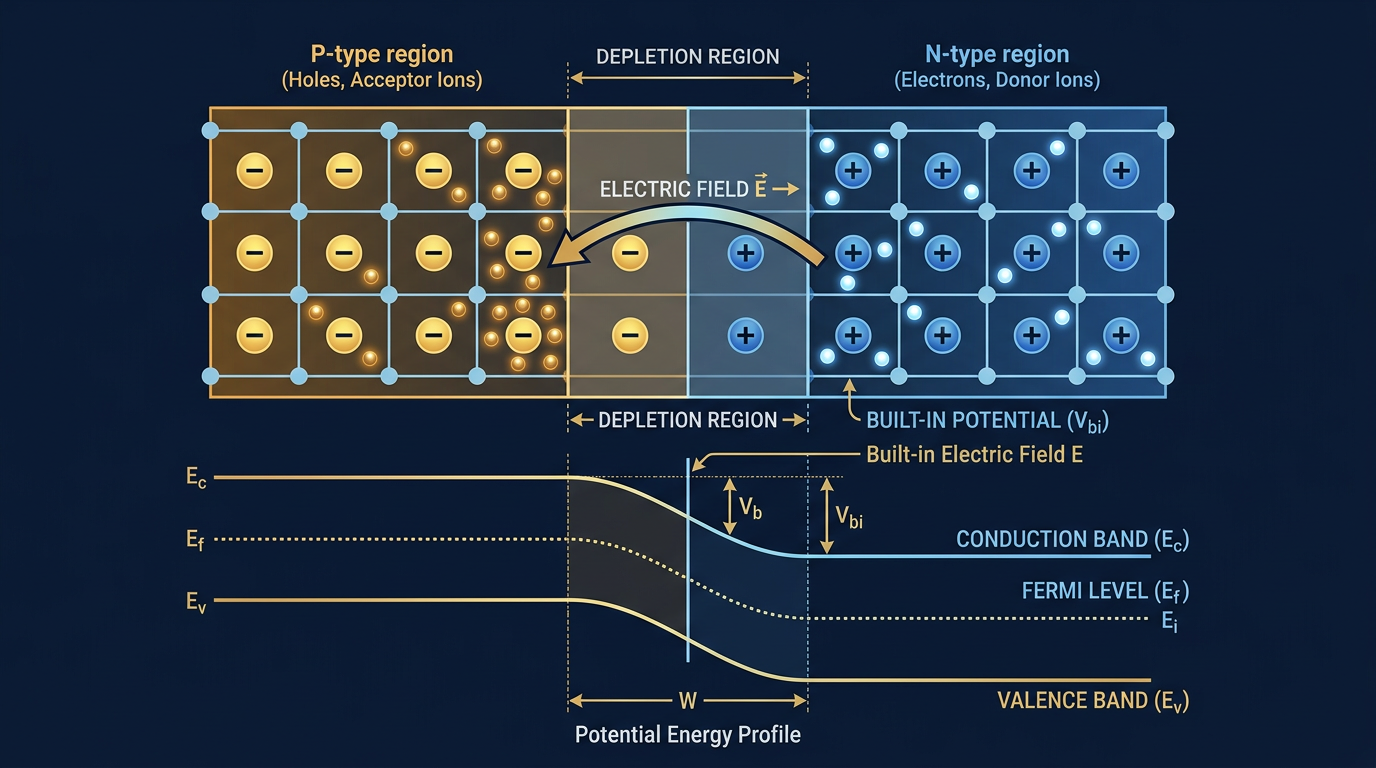
Junction Dynamics — Depletion Region & Barrier Field
Barrier field sweeps minority carriers across junction
Electrons → N-side, Holes → P-side
Prevents majority carrier flow (barrier)
Built-in Potential
Space Charge Region
Energy Bands
Output Characteristics —
Voc and Isc Under Illumination
Open-Circuit Voltage (Voc)
0.6 V
Voltage across cell terminals when no external load is connected (I = 0)
Voc = (kT/q) · ln(Iph/I0 + 1)
Determined by junction quality and recombination rate
Short-Circuit Current (Isc)
40 mA/cm²
Current when terminals are short-circuited (V = 0)
Directly proportional to incident photon flux and cell area
Isc ∝ irradiance G
AM1.5G, 1000 W/m², 25°C
η = Pmax / Pin = (Voc × Isc × FF) / Pin
V-I Curve Analysis — Maximum Power at the Knee
Voltage V (volts)
Current I (mA/cm²)
P_max = V_mp × I_mp
Maximum Power Point (MPP)
Fill Factor (FF)
FF = P_max / (V_oc × I_sc)
Dark Curve (No Illumination)
Operating at knee =
Maximum power extraction
Photovoltaic Efficiency Analysis
Applications & Engineering Constraints
Key Applications
Satellite Power Systems
High Eg materials (GaAs) preferred for space — radiation hardness, high efficiency at lower temperatures, no atmospheric absorption losses
Terrestrial Solar Farms
Silicon dominates due to low cost, mature fabrication, Eg = 1.12 eV well-matched to AM1.5 solar spectrum
Portable & Consumer Electronics
Thin-film CdTe/InAs used for flexible, low-cost applications
Engineering Constraints & Trade-offs
GaAs:
2× higher efficiency than Si but 100× higher cost
InAs (Eg=0.36eV):
captures IR but high dark current → low Voc
Silicon:
best cost-to-efficiency ratio for terrestrial use
Recombination losses limit practical efficiency (Shockley-Queisser limit ~33%)
Encapsulation & thermal management critical for longevity
Shockley-Queisser Theoretical Limit: ~33% for single-junction cells
- photovoltaics
- semiconductor-engineering
- solar-cells
- physics
- p-n-junction
- sustainability
- engineering